


The evolution and revolution of all modern technologies depend on the improvement of existing materials and the development of new materials: information processing and storage require materials that can transfer data at greater speeds and store data in smaller dimensions; transport requires materials that can withstand higher mechanical and thermal loads; environmental protection requires materials that can remove pollutants from air, water, and soil; energy requires materials that can convert solar radiation and fossil fuel efficiently into electricity; human health requires materials that can diagnose and treat different diseases. The research in our group thus focuses on the development of new materials and devices that can enable the evolution and revolution of our modern technologies. In particular, we are currently exploring the design and synthesis of two types of materials: organic-inorganic hybrid nanostructured materials and nanoscale materials. We will study their fundamental physical and chemical properties, with an emphasis on their electronic and optical properties, and fabricate novel electronic and photonic devices on different length scales (nanoscopic, microscopic, and macroscopic scales), depending on the specific type of devices.
When noble metal nanocrystals are assembled close to each other, their localized surface plasmon resonances are coupled together. The plasmon coupling gives rise to many interesting properties, which are useful for performing plasmon-enhanced spectroscopy, fabricating ultrasensitive devices, and creating artificially engineered metamaterials.
The spacing at which the plasmon resonance coupling between metal nanocrystals is on the order of a few tens of nanometers. The extent of the plasmon coupling generally decays exponentially as the spacing is increased. Therefore, to achieve the plasmon coupling, we need to develop methods to bring metal nanocrystals close to each other. Lithographical methods can give spacings down to about 10 nm. Below 10 nm, chemically or biologically assembling methods will have to be employed. We will develop chemical methods for the assembly of metal nanocrystals in solutions, on planar substrates, and in three dimensions. The assembly will be explored at different length scales, including dimers, oligomers, and macroscopic superstructures, either periodically or nonperiodically.
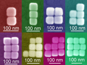
Gold nanocube clusters
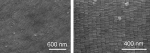
Nematic and smectic gold nanorod superstructures
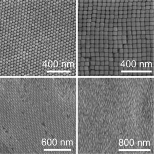
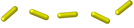
Shape-dependent gold nanocrystal superstructures
Metal nanocrystals exhibit fascinating size- and shape-dependent optical properties, which results from the surface plasmon resonance, where electrons oscillate in response to the alternating electric field of incident light. Only gold, silver, copper, and the alkali metals possess the surface plasmon resonance in the visible spectral region. Spherical metal nanocrystals exhibit only one plasmon band, while ellipsoidaland rod-like metal nanocrystals exhibit two distinct plasmon bands, which are related to transverse and 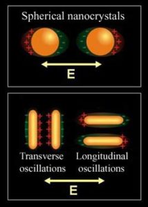 longitudinal electron oscillations (right picture). The longitudinal oscillation is very sensitive to the aspect ratio of metal nanocrystals, so that slight deviation from spherical geometry can lead to dramatic color changes.
We will focus on gold nanocrystals because of their well-developed chemical synthesis and surface functionalization. Their longitudinal plasmon resonance wavelength can be tuned via the control of their aspect ratio from the visible to the infrared spectral regions. Gold nanocrystals exhibiting such a wide spectral range of optical response are excellent components that can be used in the synthesis of organic-inorganic hybrid nanoparticles, the construction of organic-inorganic hybrid materials, and the fabrication of a variety of sensing devices. The hybrid nanoparticles and materials containing gold nanocrystals will exhibit remarkable optical and optoelectronic properties.
Coming up soon.
The localized surface plasmon resonance arises from electron oscillations in noble metal nanocrystals. Electrons are negatively charged. When two nanocrystals are placed adjacent to each other, the electron oscillation in one nanocrystal will induce the electron oscillation in the other nanocrystal. The plasmon resonances of the two nanocrystals are then coupled together. The plasmon resonance coupling is expected to depend on the parameters such as the nanocrystal spacing, shape, relative orientation, the surrounding environment, the number of nanocrystals, etc. Because the local electric field enhancement in the gap region is usually much larger than that associated with isolated nanocrystals, the gap regions in the plasmon-coupled nanocrystals usually function as hot spots for enhancing a variety of optical signals, such as Raman scattering, fluorescence/luminescence, absorption, and nonlinear signals. Moreover, the assemblies of metal nanocrystals can exhibit collective properties that are nonexistent with isolated ones. For example, when metal nanocrystals are ordered periodically, diffraction can come into play.

Plasmon coupling between metal nanospheres
Plasmon coupling between metal nanorods
We are interested in understanding the plasmon coupling properties at different length scales, ranging from dimers through oligomers to macroscopically ordered assemblies and developing plasmon-based optical devices, such as subwavelength waveguides, superlenses, and switches.
Coming up soon.